Introduction of Teacher Prof. Yu Zhu Gao studied for 5 years and got the doctor degree in electronic engineering (PhD), in Shizuoka University, Japan, 2002. During doctor course, Gao et al. found a modified liquid phase epitaxy (LPE) method named melt epitaxy (ME). InAsSb thick films with cutoff wavelengths of 8-12 µm were grown on InAs and GaAs substrates by melt epitaxy. The thickness of the epilayers reached 100 mm. This thickness effectively suppressed the affection of the lattice mismatch, thus crystal quality of long wavelength InAsSb materials has been improved. Van der Pauw measurements showed that 300 K electron mobilities of InAsSb thick layers are higher than 50000 cm2/Vs with carrier densities of (1-3) ´ 1016 cm-3. (1) Found melt epitaxyand published papers in Japan: [1] Y. Z. Gao and T. Yamaguchi, Liquid Phase Epitaxial Growth and Properties of InSbBi Films grown from In, Bi, and Sn Solutions, Crystal Research and Technology, 1999, 34 (3): 285 - 292. [2] Y. Z. Gao, X. Y. Gong, H. Kan, M. Aoyama, and T. Yamaguchi, InAs1-ySby Single Crystals with Cutoff Wavelength of 8-12 µm Grown by a New Method, Japanese Journal of Applied Physics, 1999, 38 (4A): 1939 - 1940. [3] Y. Z. Gao, H. Kan, J. I. Murata, M. Aoyama, and T. Yamaguchi, High Purity InxGa1-xSb Single Crystals with Cutoff Wavelength of 7-8 µm Grown by Melt Epitaxy, Journal of ELECTRONIC MATERIALS, 2000, 29 (10): L25 - L27. [4] Y. Gao, H. Kan, and T. Yamaguchi, The Improvement of Low Temperature Mobility of InAs0.04Sb0.96 Epilayers with Cut Off Wavelength of 12.5 µm by Annealing, Crystal Research and Technology, 2000, 35 (8): 943 - 947. [5] Y. Z. Gao, H. Kan, M. Aoyama, and T. Yamaguchi, Germanium- and Zinc-Doped P-type InAsSb Single Crystals with a Cutoff Wavelength of 12.5 µm, Japanese Journal of Applied Physics, 2000, 39 (5A): 2520 - 2522. [6] Y. Z. Gao, H. Kan, F. S. Gao, X. Y. Gong, and T. Yamaguchi, Improved purity of long-wavelength InAsSb epilayers grown by melt epitaxy in fused silica boats, Journal of Crystal Growth, 2002, 234: 85 - 90. InAsSb thick films grown on GaAs substrates by melt epitaxy: Y. Z. Gao, X. Y. Gong, Y. H. Chen, and T. Yamaguchi, High Quality InAs0.04Sb0.96/GaAs Single Crystals with a Cutoff Wavelength of 12 μm Grown by Melt Epitaxy, Proceeding of SPIE, 2006, 6029: 357-363. (2) A letter of Prof. Robert Prof. Robert in Stanford University wrote a letter to Gao in 2001. He is an editorial board of Journal of Crystal Growth. “In the opinion of the reviewers, melt epitaxy as invented by GAO et al. is an important new development for liquid phase epitaxy.” (3) Melt epitaxy and InAsSb thick layers are in a book published by WILEY M. Mauk, Chapter 12.Liquid Phase Epitaxy: A Survey of Capabilities, Recent Developments and Specialized Applications, inLiquid Phase Epitaxy of Electronic, Optical and Optoelectronic Materials (eds P. Capper and M. Mauk), 2007, John Wiley & Sons, Ltd, Chichester, UK(Print ISBN: 978-0-470-85290-3).
(4) Patents Japan Patent No. 2000-86379 China Patent No. ZL201310397546.0, No. ZL200410099025.8
(5) IEEE Membership Gao is an IEEE Membership (IEEE Membership Number: 94891511).
(6) Visiting Professor After returned to China, Shizuoka University, Japan invited Gao to work as a Visiting Professor for half a year in 2011.
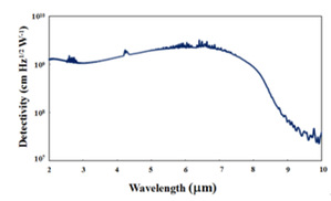
(7) Uncooled long wavelength InAsSb photodetectors fabricated by melt epitaxy High sensitivity uncooled InAsSb photoconductors with long wavelength were successfully fabricated. The detectorsare based on InAsSb thick epilayers with the thickness of 100µmgrown on InAs substrates by melt epitaxy. Immersion lenses were set on the devices. At room temperature (295 K), the photoresponse wavelength range is 2-10 µm. The peak detectivities D* (6.5 µm, 800) arelarger than 1.0 × 109 cm Hz1/2 W-1. The response time is 10-1µs, which is at least three orders of magnitude faster than heat detectors. [1] Y. Z. Gao, X. Y. Gong, G. H. Wu, Y. B. Feng, T. Makino, and H. Kan, Uncooled InAsSb Photoconductors with Long Wavelength, Japanese Journal of Applied Physics, 2011, 50 (6): 060206-1–060206-3. [2] Yu-zhu Gao, Xiu-ying Gong, Guang-hui Wu, Yan-bin Feng, Takamitsu Makino, Hirofumi Kan, Tadanobu Koyama, and Yasuhiro Hayakawa, InAsSb thick epilayers applied to long wavelength photoconductors,International Journal of Minerals, Metallurgy, and Materials, 2013, 20 (4): 393-396. [3] Y. Z. Gao, X. Y. Gong, Z. T. Chen, M. Niigaki, T. Koyama and Y. Hayakawa, Laser scanning confocal microscopy observations of InAsSb thin and thick epilayers [J]. Proceeding of SPIE, 2022, 12166: 1216619-1-1216619-7. 
At 295 K, spectral photoresponse of an InAs0.05Sb0.95 photoconductor with Ge immersion lens
|

